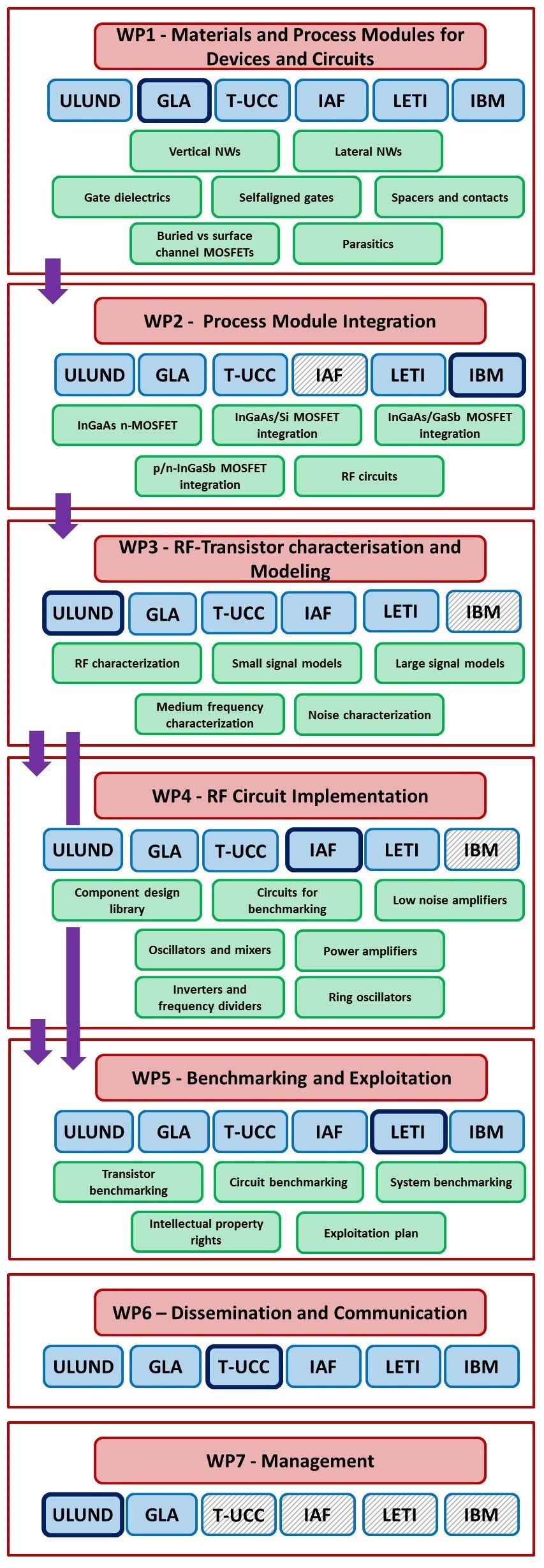
The INSIGHT project is divided into seven work packages to facilitate the execution of the work.
In WP1 we develop and optimize Materials and Process Modules for Devices and Circuits
- III-V Nanowire Formation and Integration on Si
- Gate Stack optimization
- Spacers and low resistance source/drain contacts
In WP2 we establish Process Module Integration based on modules developed in WP1.
- Process compatibility specification for hybrid, dual-channel, and single-channel RF platforms
- Optimization of InGaAs n-FET for improved RF performance
- Fabrication of co-integrated n-InGaAs/p-Si hybrid RF circuits
- Fabrication of co-integrated n-InGaAs/p-GaSb devices for dual-channel RF circuits
- Fabrication of n-GaInSb/p-GaInSb devices for single-channel RF circuits
In WP3 we perform Nanowire MOSFET RF-transistor characterization
- n-type and p-type transistor small signal model extraction
- Compact large signal modelling
- Transistor border trap evaluation: 1/f noise, gm(ω) and hysteresis
- RF Noise characterization
In WP4 we design, fabricate and characterize III-V Nanowire MOSFET circuits
- Passive and active component design library
- Circuits for on-wafer benchmarking analog millimeter-wave frequency performance metrics
- Circuits for on-wafer benchmarking complementary logic functions
In WP5 we benchmark the INSIGHT performance against competing
technologies and we develop the IPR strategy and the exploitation plan
- Transistor-level benchmarking
- Circuit-level characterisation and benchmarking
- System-level characterisation and benchmarking
- Intellectual Property Rights
- Exploitation Plan and Activities
In WP6 we focus on the channels for dissemination of the project aims and research achievements to groups outside the consortium, covering:
- Non-technical audience
- Industry
- Scientific Community
In WP7 we handle management.
|

|

