Technology Platforms
INSIGHT is aiming to provide three distinct RF CMOS platforms,
each ready at different times in the project.
|
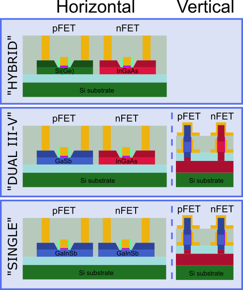
The first is an n-InGaAs/p-Si platform that we call “hybrid-channel”, and will be available already after the first year. We here utilize available nanowire n-MOSFET technology at the start of the project to rapidly demonstrate RF-circuit functionality and evaluate circuit performance. The second platform is an n-InGaAs/p-GaSb platform on Si that is called “dual-channel”. This platform evaluates the viability of full-III-V RF CMOS integrated on Si, and will also utilize the further optimized InGaAs n-MOSFETs to achieve high performance. The third platform is a more exploratory n-GaInSb/p-GaInSb “single-channel” platform, which if successfully implemented has the advantage of providing simplified CMOS processing due the usage of a single material. |
 |
|
These three tracks will build on available nanowire MOSFET technology and utilize various parts of the developed materials and processes within INSIGHT, while providing DC and RF device data and circuits for model development and advanced circuit characterization. Device modeling, measurement techniques and circuit implementation will be started directly utilizing already existing nanowire technology inside INSIGHT. As the technology platforms mature, these will be included in the circuit design effort. |
|
